
By Luigi Fragale
In this blog post, we will demonstrate how to prepare the target and perform a fault injection attack to bypass the Read Out Protection, a security feature developed by STMicroelectronics to protect firmware and sensitive customer data. We will guide you through the steps required to successfully circumvent it using the Voltage Fault Injection technique to access the firmware and any secrets it may contain. The illustration was carried out on the STM32F401CC microcontroller; therefore, conclusions and observations are only applicable to this specific product.
Fault Injection - Brief Summary
Before we dive deep into the subject, some context about the technique was used in this project:
Fault injection is a deliberate technique used to introduce errors into a system to assess its resilience and reliability. Initially developed for testing, engineers induced faults to evaluate system reliability and response. Over time, the technique transitioned into software testing allowing testers to simulate faults within software applications, such as memory corruptions or invalid inputs, ensuring that software systems can handle unexpected conditions gracefully.
Security engineers now employ fault injections to uncover vulnerabilities within systems, simulating potential attack vectors to identify weaknesses that malicious actors might exploit. On the other hand, attackers may use fault injection techniques to compromise systems.
Faults can be introduced through various methods, including, but not limited to:
- Hardware Fault Injection: Physically altering hardware components or subjecting them to extreme conditions to induce faults.
- Software Fault Injection: Modifying code, manipulating memory, or intercepting system calls to assess software robustness.
- Network Fault Injection: Simulating network disruptions, such as packet loss or delays, to evaluate the robustness of network protocols and distributed systems under adverse conditions.
The most common hardware fault injection techniques are the following:
- Clock Fault Injection: This technique involves manipulating the clock signal of a device to induce faults, caused by unexpected changes in the clock's timing. It's possible to cause the system to misinterpret instructions or process data incorrectly. Such disruptions can lead to bypass security features or leak sensitive memory content.
- Electromagnetic Fault Injection (“EMFI”): EMFI uses electromagnetic pulses to disrupt the normal operation of electronic components. By directing controlled electromagnetic interference at specific parts of the MCU, testers can induce faults that reveal vulnerabilities in hardware design or implementation. This method is particularly useful and very powerful.
- Voltage Fault Injection (“VFI”): The VFI approach involves altering the supply voltage of a device to create faults. By either cutting off or decreasing the voltage for a small amount of time, it's possible to cause malfunctions in the system's behavior. Such voltage variations can lead to data corruption or misinterpreted instructions.
These fault injection methods are essential tools in hardware security, enabling engineers to identify and address potential weaknesses before they can be exploited.
Read Out Protection (RDP)
RDP is a security feature implemented by STMicroelectronics and used in STM32 series microcontrollers to prevent unauthorized access to the device's internal memory contents. This mechanism safeguards intellectual property and sensitive data by restricting external read operations. Among other security features, this is specifically designed to prevent external access to the flash memory. (i.e., a user attempting to read the memory using JTAG or SWD debug interfaces as well as the STM32 system bootloader).
“Readout Protection, or RDP is a global mechanism that prevents external read access to Flash memory, backup SRAM and registers. An external access can be gained by using a JTAG connector, a Serial Wire port or boot software embedded in SRAM. Three levels of RDP protection are defined from level 0, which offers no protection at all, to level 2 which has full and permanent protection. [...] When first RDP level, Level 0, is set, the device has no protection. All read or write operations (if no write protection is set) on the Flash memory or the backup SRAM are possible in all boot configurations (Flash user boot, debug or boot from RAM). Option bytes are also changeable in this level.” (Ref: STM32 System Memory Protections )
RDP Levels:
- Level 0: The factory default level, no security protection is provided.
- Level 1: Read protection is set for the Flash memory, the backup SRAM, and the backup registers. In this level, protected memories are only accessible when booting from User Flash memory. Whenever a debugger access is detected or boot is not set to a Flash memory area, any access to the protected memories generates a system hard fault which blocks all code execution until the next power-on reset
- Level 2: All Level 1 protections, plus no SWD/JTAG connection possible. In this level it is not possible to jump into the system bootloader, no reverting possibility, and option bytes can no longer be changed.
ST provides also many other security features depending on the chosen product, several papers can be found on the wiki.
STM32 Bootloader
STM32 microcontrollers provide multiple methods for accessing flash memory, ensuring flexibility in managing embedded applications. These methods can be utilized either through the hardware debug interfaces or the system bootloader, a built-in feature present in nearly all STM32 devices in a dedicated memory partition (ex. 0x1FFF0000). The system bootloader facilitates communication with the STM32 device using various protocols, enabling users to perform operations such as programming, erasing, or reading memory sectors. Supported protocols include USB, SPI, UART, and others.
Below is an overview of the commands accessible via the UART interface:
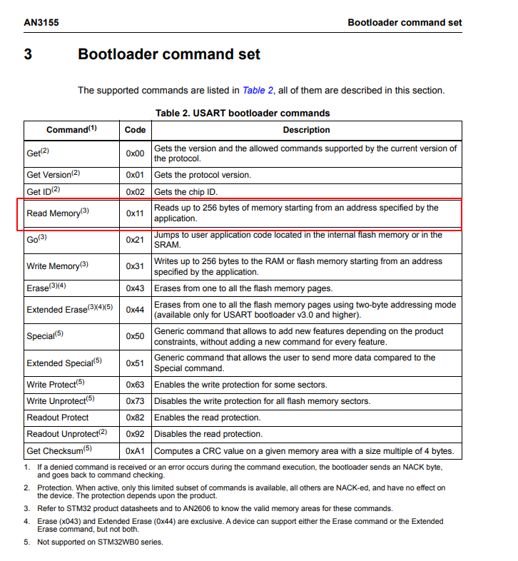
When no protection mechanisms are enabled, the 0x11 read command successfully retrieves 256 bytes from a specified page address via the UART interface. However, when RDP is activated, this operation is effectively blocked, ensuring the confidentiality of the device's memory contents.
To gain insights into this feature’s underlying implementation on the target, reverse-engineering approach was applied to the system bootloader. This analysis aims to better understand the mechanisms enforcing the RDP mechanism on the target.
The system bootloader can be extracted through the JTAG port by reading the system memory section and then loaded into a disassembler (like Ghidra).
By examining the bootloader's disassembled code, it can be observed how incoming commands are parsed and processed. The following screenshot provides a closer look at the parsing logic:
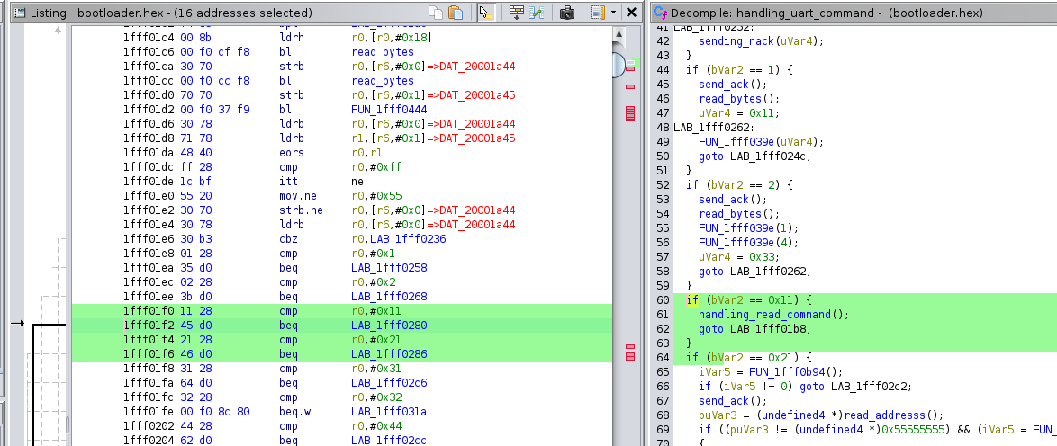
The function responsible for handling memory access performs a critical check to determine whether the RDP mechanism is enabled:
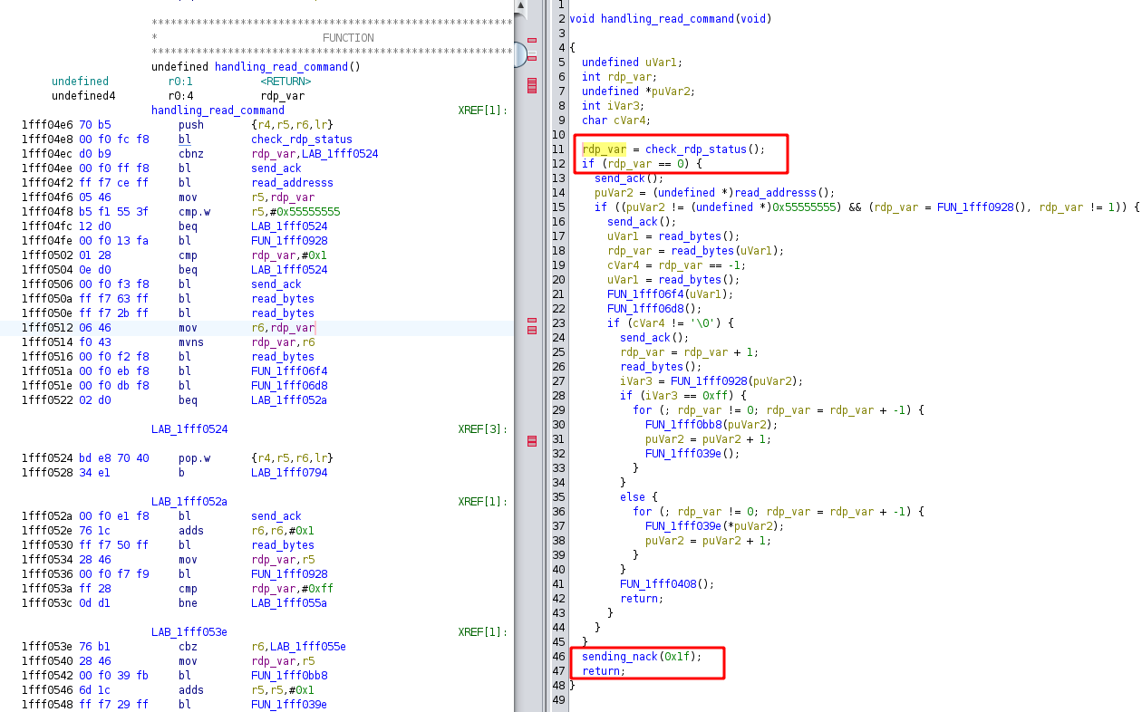
This behavior was verified by observing the value read immediately before the operation. Specifically, the highlighted memory address, 0x40023C14, indicates that the system checks the RDP status:
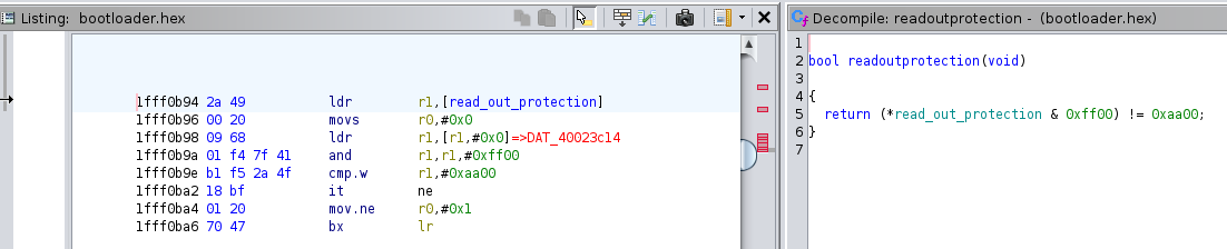
From this analysis, it can be concluded that one of the paths to circumvent the RDP protection mechanism is to target the conditional logic of the highlighted IF statement.
Environment Setup
The environment for this demonstration was deployed with the following devices and tools:
- STM32F401CC Developer Board: Used as the primary target for testing the bootloader and ROP implementation.
- CW1173 ChipWhisperer-Lite: A hardware security tool employed for fault injection and side-channel analysis.
- USB-UART TTL Converter: Facilitates communication between the host system and the STM32 device via the UART interface.
- ST-Link Programmer: Used for programming the STM32 device and configuring ROP settings
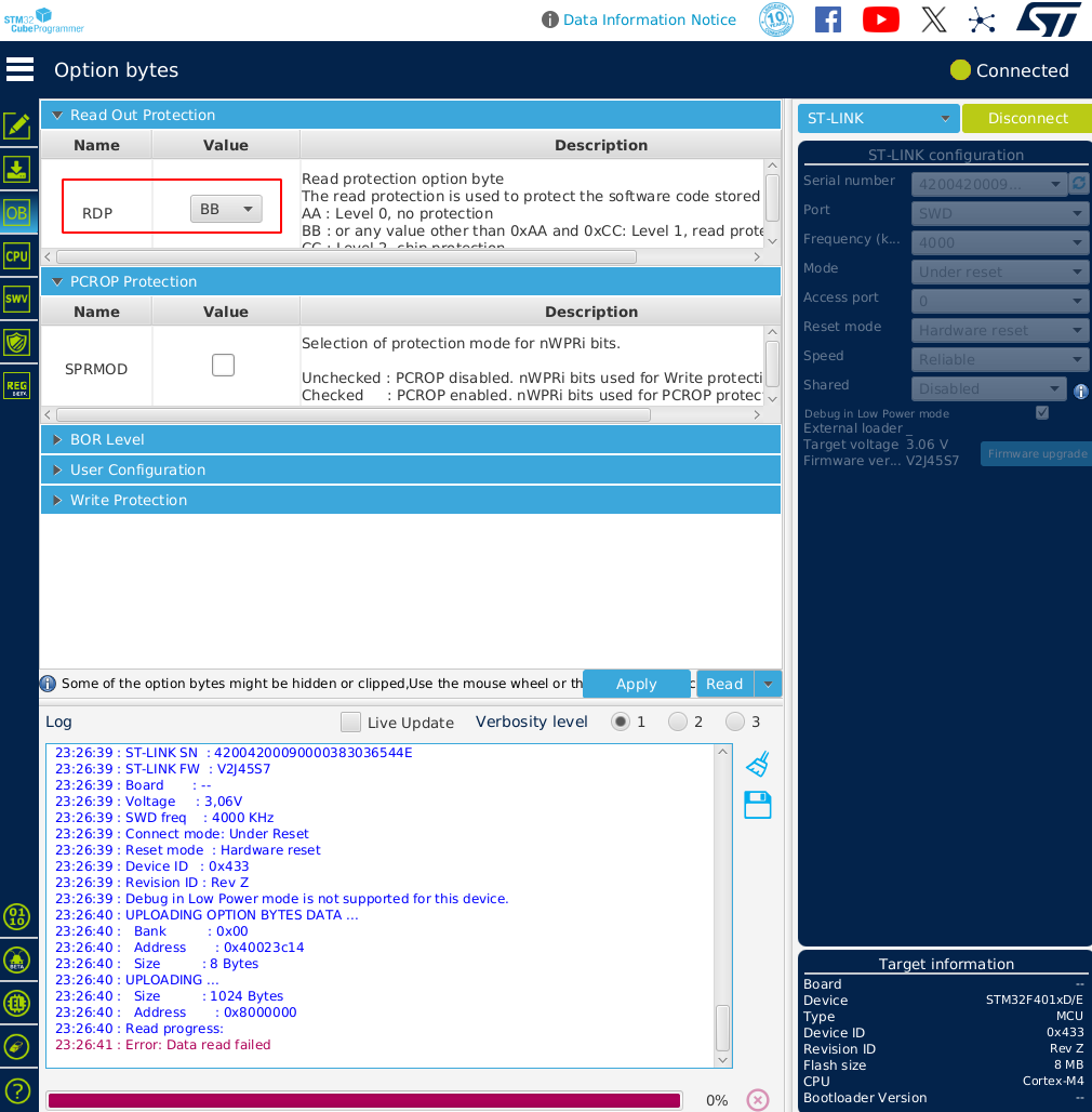
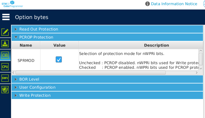
The STM32 device was programmed with dummy firmware for testing purposes, and the RDP was enabled. The configuration settings are illustrated in the image below:
Before initiating the attack, it is important to determine the optimal timing and technique for glitching the device.
The selected method for this demonstration is VFI. This approach involves briefly reducing the device's power supply, creating conditions that may cause the device to skip instructions or read malformed data. Ideally, the glitch is applied at the precise moment the device performs its RDP check, potentially bypassing the protection mechanism.
To generate an effective VFI, it is essential to:
- Analyze the Target Device: Identify and remove components that may disrupt the glitch, such as voltage regulators, bypass capacitors, or any stabilization circuitry.
- Understand the Power Domain: Gain a detailed understanding of the device’s power supply paths to pinpoint the optimal injection point.
The power supply schema for the STM32 device is shown below. The red rectangular box highlights all the components inside the MCU.
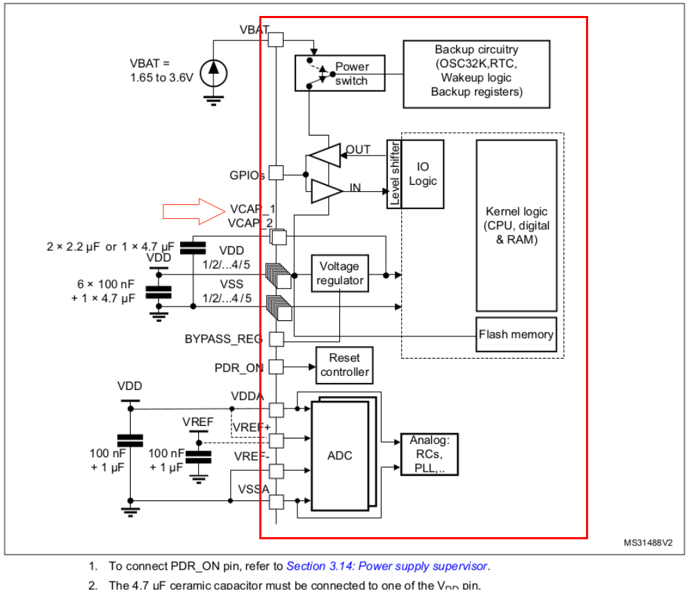
As shown, all the accessible VDD lines going to the CPU are routed through an internal voltage regulator within the System-on-Chip (SoC). However, the VCAP_1 and VCAP_2 pins are directly connected to the CPU. This direct connection makes them ideal candidates for precise VFI.
Voltage Fault Injection (VFI)
As previously mentioned, VFI is recognized as a particularly powerful technique that is widely employed by testers during security assessments of devices. This technique is utilized because power supply lines are generally accessible in all devices, which creates an easily approachable injection point, although exploitation is not always possible. Furthermore, IoT devices are designed to function within specific operating conditions. Functionality is typically guaranteed by manufacturers exclusively under these predetermined settings 'General operating conditions'.

These are the conditions under which proper device operation is guaranteed. However, when these specified conditions are not met, device operations may become unpredictable, or the device might simply stop functioning. This can be leveraged using the VFI technique to modify instructions, corrupt data memory, or flip bits.
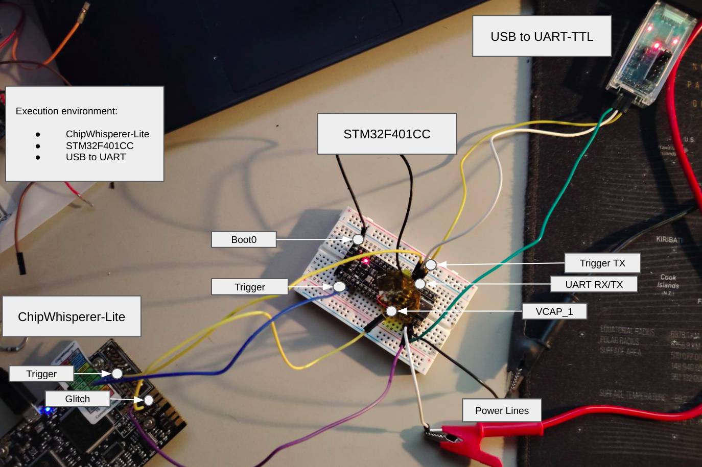
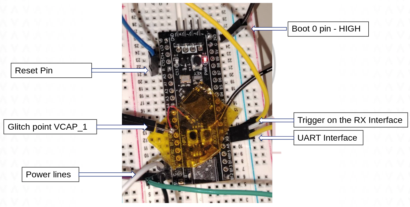
Hardware Preparation
To set up the environment for the attack, the following modifications were made to the target device:
- VCAP_1 Pin: A cable was soldered to the VCAP_1 pin to facilitate VFI. Relevant bypassing capacitors were desoldered.
- BOOT0 Pin: The BOOT0 pin was manually configured to a HIGH state, ensuring that the device boots directly from the system bootloader upon each reboot.
- USART Interface: The USART interface was connected to a USB-UART TTL Converter for communication with the device. The TX line was looped back into the triggering pin (TIO4) of the ChipWhisperer, allowing for synchronized control and precise fault injection during the attack.
- RESET Pin: The RESET pin was connected to the ChipWhisperer TIO3.
The diagram below illustrates the hardware setup used for this process:
The external USB-UART TTL Converter is used in this setup because the ChipWhisperer Lite board does not support UART parity configuration, which is necessary for reliable communication with the bootloader.
Execution
With the hardware setup properly configured, the next step is to determine the optimal glitch parameters.
Before targeting the RDP function within the bootloader, it's important to identify the minimum glitch settings needed to induce a successful fault that causes the device to skip instructions. A simple routine like the one below serves as a useful starting point for experimentation:
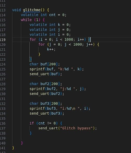
This routine is a good example for experimenting with various glitch parameters, allowing for the observation of their effects and optimizing the fault injection process.
During the glitching sessions (shown below), values were observed to be corrupted while the device continued to operate normally. This indicates that valid parameters for a successful glitch are close to being found. The tool used to generate the glitches is the Chipwhisperer Lite board https://rtfm.newae.com/Capture/ChipWhisperer-Lite/.
With the key parameters repeat, width, offset, and clock frequency identified, the attack can now proceed (These parameters can be set using the Chipwhisperer Python API. For further details, please refer to https://chipwhisperer.readthedocs.io/en/latest/scope-api.html).
Another critical parameter to consider is the ext_offset. This value defines the waiting period before the glitch is triggered and is expressed in clock cycles as 1/clkfreq. To ensure the glitch occurs at the right moment, the ChipWhisperer trigger pin was connected to the USART_TX line of the USB-to-UART TTL converter. However, further fine-tuning is required to determine the precise delay (or waiting time) before initiating the glitch to ensure it aligns with the moment when the target received the 0x11 read command.
During testing, finding the right ext_offset introduced several challenges. This will be further discussed in the closing section.
Determine the ext_offset
A logic analyzer was employed to measure the timing of the transmission and reception of the 0x11 read command. The software provided with the logic analyzer includes a precise timing measurement feature. This feature allows for accurate measurement of the exact time intervals between when the 0x11 command is transmitted and when the instruction is fully received and processed, helping to determine the ideal moment for the glitch injection.

Various measurements were taken, leading to the following time estimation:
- Read Memory request command issue timing:
182.300 µs - Read Memory response command issue timing:
196.800 µs
From these values, the minimum waiting time before issuing the glitch is calculated as follows:
- Clock cycle duration:
1/clkfreq== 10ns - Minimum Waiting time:
182300/10 = 18230 clock cycle.
Thus, the ext_offsetvalue, which defines the number of clock cycles before initiating the glitch, should be set to a minimum of 18230 clock cycles to trigger the fault at the optimal moment.
Glitch Session
After several iterations of fine-tuning and adjustments, the optimal ext_offset parameter was found to be between 18300 and 18370 clock cycles. With this adjustment, the script is now able to run successfully and consistently glitch the desired operations.
Full script can be found in this repository.
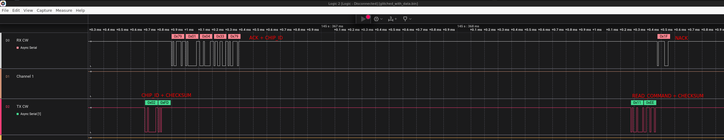
$ python3 glitchstm32f401.py

cwlite Device

[...]

Got ack
Can read the memory: 1.953125 10.15625 2 18365
Sending memory address :134225920 0800200028
Result 1f1f
Glitched
b'y'

Got ack
Can read the memory: 1.953125 10.15625 2 18313
Sending memory address :134225920 0800200028
Result 1f1f
Glitched
b'y'

Got ack
Can read the memory: 1.953125 10.15625 2 18313
Sending memory address :134225920 0800200028
Result 1f1f1f
Glitched
b'y'
Got ack
Can read the memory: 1.953125 10.15625 2 18320
Sending memory address :134225920 0800200028
Result 79
Ack, read the memory address: 0800200028

Result: 794346e318c7f898304b4645eb0303c7f89c30d7f8f4305b680022c7f89030c7f894204ff000024ff00003d7e9244529468b00214643ea917321468a00d7e92601fef7daf802460b46604ba3fb02235b091c01d7f8fc300022c7f88830c7f88c20d7e9228942464b469118b9615b41fb61d7e9062341465118396149464b417b614ff000024ff00003d7e904ab5946cb00514643ea51735146ca0010461946034642469b18c7f880304b460a4642eb0303c7f88430d7f8f4305b680022bb67fa674ff000024ff00003d7e91e8949468b00414643ea917341468a00d7e92001fef78bf802460b461146384ba3fb01235b09642202fb03f3cb1a1b013233334aa2

Bytes to read: 794346e318c7f898304b4645eb0303c7f89c30d7f8f4305b680022c7f89030c7f894204ff000024ff00003d7e9244529468b00214643ea917321468a00d7e92601fef7daf802460b46604ba3fb02235b091c01d7f8fc300022c7f88830c7f88c20d7e9228942464b469118b9615b41fb61d7e9062341465118396149464b417b614ff000024ff00003d7e904ab5946cb00514643ea51735146ca0010461946034642469b18c7f880304b460a4642eb0303c7f88430d7f8f4305b680022bb67fa674ff000024ff00003d7e91e8949468b00414643ea917341468a00d7e92001fef78bf802460b461146384ba3fb01235b09642202fb03f3cb1a1b013233334aa2

Glitched
b'y'
Got ack
Can read the memory: 1.953125 10.15625 2 18332
Sending memory address :134226176 0800210029
Result 79
Ack, read the memory address: 0800210029

Result: 7903235b0903f0f0031c44d7f8fc3000223b677a67d7e91c8942464b469118b9605b41fb60d7e9022341465118396049464b417b604ff000024ff00003d7e900ab5946cb00514643ea51735146ca0010461946034642469b18bb664b460a4642eb0303fb66d7f8f4305b6800223b667a664ff000024ff00003d7e9188949468b00414643ea917341468a00d7e91a01fef733f802460b460d4ba3fb02135b09642101fb03f3d31a1b013233084aa2fb03235b0903f00f02d7f8f4301b6822449a6000bf07f58077bd46bde8b08f1f85eb5102440346934200d1704703f8011bf9e770b50d4d0d4c641ba4100026a64209d10b4d0c4c00f018f8641ba4100026a6

Bytes to read: 7903235b0903f0f0031c44d7f8fc3000223b677a67d7e91c8942464b469118b9605b41fb60d7e9022341465118396049464b417b604ff000024ff00003d7e900ab5946cb00514643ea51735146ca0010461946034642469b18bb664b460a4642eb0303fb66d7f8f4305b6800223b667a664ff000024ff00003d7e9188949468b00414643ea917341468a00d7e91a01fef733f802460b460d4ba3fb02135b09642101fb03f3d31a1b013233084aa2fb03235b0903f00f02d7f8f4301b6822449a6000bf07f58077bd46bde8b08f1f85eb5102440346934200d1704703f8011bf9e770b50d4d0d4c641ba4100026a64209d10b4d0c4c00f018f8641ba4100026a6
[...]
Subsequently, the firmware can be read, obtaining all the secrets in it:
$ echo -n 7905d170bd55f8043b98470136eee755f8043b98470136f2e7e0220008e0220008e0220008e4220008f8b500bff8bc08bc9e467047f8b500bff8bc08bc9e46704773757065727365637265746b6579000077726f6e6721210a00000000477565737320746865206b6579210a0050617373776f726420636f7272656374210a00004c6f636b6564210a00000000476c697463686564210a00006b3a2564200000006a3a256420000000693a25640a200000476c6974636820627970617373000000000000000000000001020304060708090000000001020304fcdeff7f01000000b90100089501000840220008502200085c2200086c2200080024f400100000 | xxd -r -p

y�p�U�;�G6��U�;�G6������������FpG������FpGsupersecretkeywrong!!

Guess the key!

Password correct!

Locked!

Glitched!

k:%d j:%d i:%d

[...]
Conclusion
Glitching is inherently unpredictable and non-deterministic, with variables such as temperature, wire length, and environmental conditions significantly affecting the outcome. Several challenges were encountered, multiple instances of target were temporarily misconfigured due to glitches in unrelated memory areas. In the initial run, using a broad ext_offset range of 18230 to 19500 clock cycles produced varied responses. In many cases, it was revealed that the glitch caused both the RDP and Write Protect features to adopt random values, resulting in an unstable environment
The PCROP setting was found to be enabled after a few glitches; however, other settings were also corrupted, making the device temporarily unusable.
Overall, the process involved extensive troubleshooting, with hours spent diagnosing setup issues and refining the glitching process. In total, approximately six hours were dedicated to glitch the device and the extract the totality of the firmware.
To mitigate the risks and improve the reliability of future glitching attempts, several strategies can be employed. When designing a product, it is important to consider these types of attacks. Chip selection is crucial and plays a significant role, as many chips have built-in security mechanisms against fault injection. In more complex architecture, like Intel CPUs, dedicated circuits are involved to detect misalignment in timing. An example of such a circuit is the Tunable Replica Circuit, which helps detect multiple attacks, including clock, VFI, and EMFI.
For existing solutions, software counter measures can also be applied. Repeating critical operations multiple times and verifying the results or adding random delays before sensitive operations can further reduce the likelihood of successful attacks.
It is important to be aware of fault injection attacks and evaluate them within the threat modelling design of your product. Some devices may not have enough security measures against these new threats and successful attacks can lead to the full compromise of your products and infrastructure. Evaluating the potential threats during the product design stage can help to identify the right products for the designated business.